扫描电镜之家 » 讨论区 » 经验共享 » 资料:扫描电镜 Introduction to EBSD

采购询价

点击提交代表您同意 《用户服务协议》 《隐私政策》

 
需要登录并加入本群才可以回复和发新贴

标题:资料:扫描电镜 Introduction to EBSD

scattering[使用道具]
五级
Rank: 5Rank: 5


UID 33040
精华 11
积分 1115
帖子 460
信誉分 133
可用分 2981
专家分 196
阅读权限 255
注册 2010-1-27
状态 离线
1
 

资料:扫描电镜 Introduction to EBSD

0 Introduction

Electron Backscatter Diffraction (EBSD) is a technique which allows crystallographic information to be obtained from samples in the scanning electron microscope (SEM). In EBSD a stationary electron beam strikes a tilted crystalline sample and the diffracted electrons form a pattern on a fluorescent screen. This pattern is characteristic of the crystal structure and orientation of the sample region from which it was generated.

The diffraction pattern can be used to measure the crystal orientation, measure grain boundary misorientations, discriminate between different materials, and provide information about local crystalline perfection. When the beam is scanned in a grid across a polycrystalline sample and the crystal orientation measured at each point, the resulting map will reveal the constituent grain morphology, orientations, and boundaries. This data can also be used to show the preferred crystal orientations (texture) present in the material. A complete and quantitative representation of the sample microstructure can be established with EBSD.

In the last ten years EBSD has become a well established technique for the SEM, and obtaining crystallographic information from samples is now both routine and easy.

1. Principal system components

The principal components of an EBSD system are (Figure 1):

>>A sample tilted at 70° from the horizontal.

>>A phosphor screen which is fluoresced by electrons from the sample to form the diffraction pattern.

>>A sensitive charge coupled device (CCD) video camera for viewing the diffraction pattern on the phosphor screen.

>>A vacuum interface for mounting the phosphor and camera in an SEM port. The camera monitors the phosphor through a lead glass screen in the interface and the phosphor can be retracted to the edge of the SEM chamber when not in use.

>>Electronic hardware that controls the SEM, including the beam position, stage, focus, and magnification.

>>A computer to control EBSD experiments, analyse the diffraction pattern and process and display the results.

>>An optional electron detector mounted below the phosphor screen for electrons scattered in the forward direction from the sample.
顶部
scattering[使用道具]
五级
Rank: 5Rank: 5


UID 33040
精华 11
积分 1115
帖子 460
信誉分 133
可用分 2981
专家分 196
阅读权限 255
注册 2010-1-27
状态 离线
2


2 Pattern formation

For EBSD, a beam of electrons is directed at a point of interest on a tilted crystalline sample in the SEM (Figure 2).


Formation of the electron backscattered diffraction pattern. Electrons from a divergent source incident on crystal planes at the Bragg angle are diffracted into a pair of cones to form Kikuchi bands in the diffraction pattern.
顶部
scattering[使用道具]
五级
Rank: 5Rank: 5


UID 33040
精华 11
积分 1115
帖子 460
信誉分 133
可用分 2981
专家分 196
阅读权限 255
注册 2010-1-27
状态 离线
3
 
2.1 About the Crystals and lattices

2.1.1 Crystal lattice

Crystalline material consists of a regular repetition of a group of atoms in three dimensional space. A crystal lattice is an infinitely repeating array of points in space.
顶部
scattering[使用道具]
五级
Rank: 5Rank: 5


UID 33040
精华 11
积分 1115
帖子 460
信誉分 133
可用分 2981
专家分 196
阅读权限 255
注册 2010-1-27
状态 离线
4
 

A crystal lattice

2.1.2 Unit cell

The unit cell of the lattice is the basic repeating unit of the lattice and is characterized by a parallelepiped with cell edge lengths a, b, c and inter axis angles α, β ,γ.


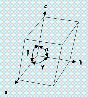
Unit cell of a lattice

2.1.3 Bravais Lattices

These unit cells can be classified as belonging to one of fourteen Bravais lattices. Each Bravais lattice belongs to one of the seven crystal systems.


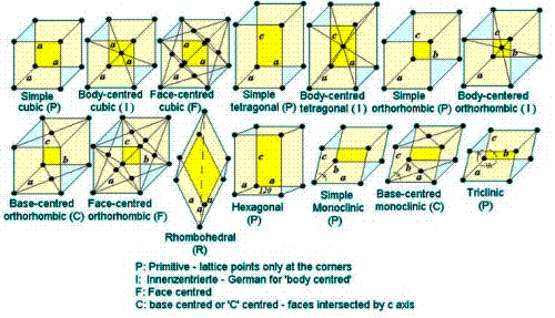
The fourteen bravais lattices

2.1.4 Motif

The motif is the group of atoms repeated at each lattice point.


Crystal structure showing a repeated atomic motif at each lattice point.
顶部
scattering[使用道具]
五级
Rank: 5Rank: 5


UID 33040
精华 11
积分 1115
帖子 460
信誉分 133
可用分 2981
专家分 196
阅读权限 255
注册 2010-1-27
状态 离线
5
 

A diffraction pattern from nickel collected at 20 kV accelerating voltage.
顶部